Electronic Circuit Design
- Subject Code :
EN8007T
Learning outcomes(LOs)
On successful completion of this test the student will partially be able to:
|
1 |
Demonstrate critical knowledge of theories, principles and concepts relating to design, building, and testing of advanced electronic circuits |
|
|
2 |
Construct and analyse an advanced electronic circuit to a given specification aided by the use of advanced software packages and electrical/electronic test/measurement equipment |
|
|
3 |
Design, build, test an environmentally friendly, sustainable, and cost effective advanced electronic circuit all in accordance with local/international standards and a given specification. |
|
Question number |
Task description |
LOs |
|
1 |
Filter Design |
1,2,3 |
|
2 |
Simulation of the designed circuits |
1,2,3 |
|
3 |
Prototyping the circuit in Breadboard/PCB |
1,2,3 |
Feedback
According to Bahrain Polytechnic policy,
- Feedback will be provided to students within 10 working days of
- Students are required to apply for a remark of any contested grading within 4 working days of receiving back their work.
- All marks/grades given are provisional and subject to change as a possible result of post moderation
Introduction
This project is worth 30% of your final grade. The project should be completed by 20.05.2026.
Deliverables
The following deliverables must be submitted by the project deadline:
- The Circuit design and simulation results using any electrical
- A filter design project
- The implemented breadboard /PCB
Project Report
Prepare a project report that outlines all the tasks listed below. Justify your selection of the electrical components and how they meet the criteria for the desired design specifications.
The report should be prepared as if it were for a supervisor at your workplace. Ensure that your report is clear and transparent.
You need to ensure the following:
- Clear Design Procedure must be used to solve tasks 1&2
- Demonstrate your results using a Bode plot of the design
- All the circuit design and simulation results should be included in the report/uploaded in the MOODLE
- Label the axes of each and every This includes attaching a figure legend when appropriate.
whats being measured and that it is not anarbitrary variable.
- Every graph must have a descriptive Label and scale allaxe saccurately.
- Number your plots and graphss equentially,g.Fig.1,2etc.
Background theory
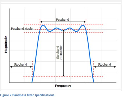
A filter is a circuit that passes certain frequency and rejects the remaining frequencies based on the type of the filter. There are five types of filters whether passive or active: low pass filter, high pass filter, band pass filter, band stop filter and all pass filters. Bandpass filter bass a band of frequencies and reject other frequencies.
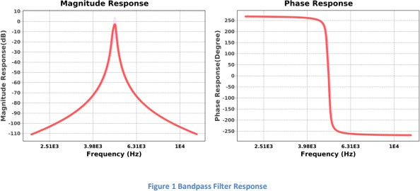
Figure 1 shows the bode plot response of bandpass filter where the magnitude (in decibels) and phase (in degrees).
Task1Design
- Design a bandpass filter that satisfies the specifications: (Note: The specifications are per group).
|
Parameters |
A |
B |
C |
D |
E |
F |
|
Gain(V/V) |
3 |
2 |
5 |
6 |
8 |
7 |
|
Pass Band Ripple(dB) |
0.5 |
1 |
0.5 |
1 |
0.5 |
1 |
|
Centre Frequency(Hz) |
150 |
100 |
200 |
150 |
200 |
100 |
|
BW(Hz) |
100 |
100 |
100 |
100 |
100 |
100 |
|
Stopband attenuation(dB) |
30 |
35 |
30 |
35 |
30 |
35 |
|
Stopband BW(KHz) |
1 |
1 |
1 |
1 |
1 |
1 |
Table1
- Select the values ofall the components in the circuit that satisfy the required design in part (a) and minimize the cost of the implementation.
Task2 Simulation and Testing
Simulate your circuit using any available simulation software then:
- Prove that the specified design parameters in Table1 are satisfied in the designed
- Plot the Bode Plot of the circuit frequency
Task3 Implementation and Verification
Implement the design on a breadboard printed circuit board (PCB) for your design. The implemented design of the Bandpass Filter will be assessed based on the following tasks.
- Prove that the specified design parameters in Table1 are satisfied in the designed
- Plot the Bode Plot of the circuit frequency
- Implementation cost and
The data from the experimental testing must be obtained and compared with the simulation data as part of your discussion of your report.

|
MARKING SCHEME |
|||
|
Criteria |
Marks |
Description |
|
|
Theoretical Design |
|||
|
Specification interpretation |
5 |
Correct identification of fc, BW, Q, filter type, order |
|
|
Order selection & justification |
5 |
Correct reasoning (Chebyshev / Butterworth, 4th order etc.) |
|
|
Design equations & calculations |
5 |
Correct formulas, steps, Q calculation, component derivation |
|
|
Component selection |
5 |
Practical standard values chosen |
|
|
Circuit Simulation |
|||
|
Correct schematic |
5 |
Proper topology and connections |
|
|
AC frequency response |
5 |
Bode plot showing center frequency & bandwidth |
|
|
Gain verification |
5 |
Gain ? specified value |
|
|
Stopband verification |
5 |
Attenuation demonstrated |
|
|
Breadboard Implementation |
|||
|
Wiring quality |
5 |
Clean layout, grounding, decoupling |
|
|
Correct component usage |
5 |
Values match design |
|
|
Functionality |
5 |
Circuit works and produces band-pass behavior |
|
|
Troubleshooting ability |
5 |
Student identifies and fixes issues |
|
|
Experimental Results &Validation |
|||
|
Measurement of fc |
5 |
Measured center frequency close to design |
|
|
Measurement of BW |
5 |
Bandwidth validated |
|
|
Comparison with simulation |
5 |
Discussion included |
|
|
Technical Report |
|||
|
Structure & formatting |
2 |
Proper sections |
|
|
Theory explanation |
4 |
Filter concept explained |
|
|
Simulation results |
3 |
Graphs properly labeled |
|
|
Hardware results |
3 |
Photos, measurements |
|
|
Discussion & conclusion |
2 |
Error analysis, learning outcomes |
|
|
References |
1 |
Proper references are given in standard form |
|
|
Viva |
10 |
||