Polymer-Mediated Enhancement of Sensitivity and Stability CHEM4021
- Subject Code :
CHEM4021
Polymer-Mediated Enhancement of Sensitivity and Stability in CNT-FET-Based DNA or Antibody Biosensors
TableofContents
TableofContents
DifferentConfigurationsofEG-FET 5
LimitationsofUnpassivatedCNT-FETs 7
- PolymersinFETG
Non-ConductivePolymers(NCPs) 11
- Materials&Methods1C
1.Introduction
Ifascientistisnotbefuddledbywhattheyre
lookingat,thentheyrenotaresearchscientist.
- NeildeGrasseTyson(1958-)
1.1.Motivation
Conventional bio-detection methods, such as optical or magnetic platforms, often fall short inmeeting the demands ofpoint-of-care (POC)applications. Despite their analytical precision, these techniques rely on labor-intensive workflows, specialized equipment, and lengthy processing times, rendering them impractical for use in decentralized or resource-limited healthcare environments. Consequently, there is a critical needtoreimaginebiosensor designprinciples, emphasizing compactform factors, rapid response times, andoperational simplicity to ensure seamless integration intoreal-worldclinicalandcommunitysettings[1].
Totranslate suchtechnologies intoeffective POCsolutions,threeinterdependent criteria must be addressed: (1) compatibility with large-scale production, (2) robust specificity for targetbiomarkers,and (3)economicviability for globaldeployment[2, 3]. Field-effect transistors (FETs)are widely regarded as an excellent foundation for creating advanced and integrated biosensor chips. Their ability to be miniaturized and produced onalargescalemakesthemparticularly appealingforsuchapplications[4- 7].
FET-basedbiosensors work by using the core functions oftransistors to detect and amplifysmallbiological orchemicalchanges,suchasmolecular interactions orshifts inionconcentrations. Thesechangesareconvertedintoelectronicsignalsthatareeasy to measure and directly linked to the presence of the target analyte in the sample[8, 9]. With the progress of nanotechnology, the performance of these biosensors has significantly improved, especially with the integration of nanomaterials into their semiconductingchannels,makingthemmoresensitiveandefficient[8,10-13].
Amongthevariousbiosensingplatforms,carbonnanotubefield-effecttransistors (CNT-FETs)haveemergedaspromisingcandidates owingtotheirexceptional electrical properties, highsurface-to-volumeratio, andexcellent biocompatibility[8,12]. However, despite their potential, CNT-FET-basedbiosensors, even after used hafnium oxide (HfO2)and photoresist passivation, often face challenges related to low sensitivityandstabilitywhichcanhindertheirpracticalimplementation[14].
One of the primary factors contributingto these limitations is the presence of leakage currents and the degradation of the passivation layer over time, leadingto adecrease in the device's performance and reliability [15]. To address these issues, explored various strategieshave beenexplored, including theincorporation ofadditional passivation layers to enhance the sensitivity and stability of CNT-FET-basedbiosensors. One promising approach involves the introduction of a polymer layer as an additional passivationlayeroverthecommonlyusedHfO2+photoresistlayeronCNT-FET[16].
The incorporation of a polymer layer as an additional passivation layer offers several advantages. First, itcaneffectively suppress leakage currents, which can interfere with the accurate detection of biomolecules by masking the desired drain current changes. Second, the polymer layer can provide enhanced stability by protecting the underlying layers fromenvironmental factors, suchasmoistureandcontaminants, whichcan degrade the device's performance over time.Furthermore, the polymer layer can be tailored toexhibit specific properties, such ashydrophilicity or hydrophobicity, which can facilitate the immobilization of biomolecules and improve the overall sensitivity ofthe biosensor [7, 17-21].
1.2.CNT-FETasBiosensors
Asdiscussed before, biosensors based on FETsare highly promising electrochemical devices. Their excellent electronic properties and ability to amplify signals make them highly sensitive and selective for detectinga wide range of biomolecules [22, 23]. The most commonFETtechnology is themetal-oxide-semiconductor FET(MOSFET), whichusesasilicon (Si)channel separated from thegatecontact byathinsilicon dioxide (SiO?) layer [24]. FETsensors come in different designs, includingback-gated (BG-FET)[25-27],dual-gated (DG-FET)[28, 29] or electrolyte-gatedFETs (EG-FETs) [9, 30, 31].
Table1:AdvantagesandDisadvantagesofdifferentconfigurationsofFETs.
|
Configuration |
Pros |
Cons |
|
BG-FET |
Simplestructure Easytofabricate |
Lower gate control efficiency Higheroperatingvoltage |
|
DG-FET |
Bettergatecontrol Loweroperatingvoltage Improvedperformance |
More complex fabrication process |
|
EG-FET |
Highsensitivityforbiosensing Lowoperatingvoltage Suitable for liquid environments |
Limited to aqueous environments Potential electrochemical reactions |
Amongthese, EG-FETsare particularly useful for biosensing. They replace the SiO? layer withanelectrolyte, suchasasolidpolymer, anion-gel, orawater-based electrolyte [9].In EG-FETswherecarbonnanotubes(CNTs) serveasthe semiconductor layer, thesedevicesarereferredtoasEG-CNT-FETs.
EGCNT-FETsoffer many benefits, includinghigh sensitivity, fast response times, the ability to work at low temperatures, and stable performance. They can also detect molecules without needing labels, making them ideal for sensing chemicals andbiologicalsubstances[32].These advantagesmakeEGCNT-FETsa key technologyfor modernbiosensors,drivingtheiruseinreal-worldapplications[1,8].
WorkingofCNTFETs
All CNTFETsshareacommon setof components:aconductivechannelmade of CNTs, source and drain electrodes, a gate electrode (positioned either above or below the channel), and a dielectric layer that electrically isolates the gate from the CNTchannel [14, 33-35]. Despite differences in structure, all CNTFETsoperate on similar principle. Thegateelectrode applies avertical electric fieldtocontrol thechargedensitywithin the CNTchannel. Simultaneously, a horizontal electric field is established between the sourceanddrainelectrodes, creatingadrivingforceforchargecarriers. Thisresultsin acurrent flow,knownasthedrain-sourcecurrent,from oneelectrode totheothervia the CNT channel.
Fig.WorkingprincipleofCNT-FET[adaptedfrom[1]]
The operationofEGCNT-FETsis basedonthe uniquebehaviorofionsinan electrolyte. When an externalvoltage (electric field)is applied,the ions in the electrolyte rearrange, forming two electric double layers (EDLs) [8, 36].These EDLsappear at the interfaces between (1) the gate electrode and the electrolyte, and (2) the CNTchannel and the electrolyte.This dual-layer formation effectively causes the bulk electrolyte to act asan insulator,enablingthetransistortofunctionsimilarlytoaconventionalFET.
As illustrated inFigure 2(a), in the absence of an applied voltage, cations (positively charged ions) and anions (negatively charged ions) remain randomly distributed within the electrolyte. Since semiconducting CNTstypically exhibit p-type behavior due to oxygen in the air acting as a natural p-dopant [37]. This means that a negative bias is generallyrequiredtoactivate(or"turnon")theCNT-FET.
Fig.[adaptedfrom[8,36]]
When a negative bias is applied between the gate and source electrodes,as shown inFigure 2(b), the electrolyte responds by forming EDLs. Cations accumulate at the interface between the gate electrode and the electrolyte, while anions gather at the interface between the electrolyte and the CNT channel. At both interfaces, a thin monolayer of ions forms, followed by a region where ion concentration gradually decreases withan exponential profile. This behavior alignswith the Stern-modified GouyChapman double layer model [38], which explains the ion distribution nearcharged surfaces.
DifferentConfigurationsofEG-FET
Researchers have investigated several designs for EGFETs,each offering distinct advantages and disadvantages. These configurations have been detailed in prior studies[9,39].Threeprimaryconfigurationsareparticularlynoteworthy:
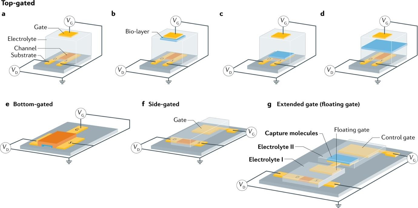
Fig.Differentarchitechure ofEG-FETs[adaptedfrom[9,39]]
- ConventionalGated(ReferenceElectrode)
This is the most established and frequently used design. It utilizes a standard reference electrode, such as Ag/AgClor a platinum wire, as the gate. This approach provides stable and reliable operation, allowingfor precise control over the gate potential. This configuration is used as gold-standard to check the performanceofnewlydevelopedconfigurations.
- Planar(orSide)Gated
In this configuration, the gate electrode is fabricated on the same plane as the source and drain contacts. This design simplifies the fabrication process. Furthermore, its compatibility with flexible substrates and the elimination of externalreferenceelectrodescanleadtoreducedmanufacturingcosts.
- ExtendedGate
Thisconfiguration separates theEGFETinto twodistinct parts: thecore transistor and a physically separate gate electrode. This separation enhances stability and reproducibility because only the sensing regionisdirectly exposedto the measurement environment.
The selection of an EGFETconfiguration is contingent upon the specific application demands, fabrication constraints, anddesired performance characteristics. Withinthe context of the present thesis, thePlanar Gated EG-CNT-FETconfiguration has been used. Forthe sake of conciseness and clarity throughout the subsequent discussion, the term'CNT-FET'is used interchangeably with'Planar Gated EG-CNT-FET'in the following sections.
LimitationsofUnpassivatedCNT-FETs
Thesedevicesoftenfaceseveralcriticalchallenges[14,15,40]:
- LeakageCurrent
Unpassivated CNT-FETsoftensuffer fromhighleakagecurrents, whichcan mask the desired signal and compromise sensingaccuracy.This issue arises from thedirect exposure ofthe device components totheelectrolyte .Theionic solution can create conductive paths between electrodes, leading tounwanted currentflowthatinterfereswiththedevice'sperformance.
- StabilityinIonicEnvironments
The performance of EG-CNTFETscan degrade rapidly when exposed to ionic solutions, a commonmedium inbiosensing applications. This instability stems fromtheinteraction between the electrolyte and the exposed CNTchannel. Ions in the solutioncan adsorbontothe CNTsurface,alteringits electronicproperties andleadingtodriftinthedevice'scharacteristicsovertime.
- Long-termReliability
Repeated ionic doping and de-doping of the CNTchannel can lead toperformance degradation over time, limitingthe device's lifespan and reliability forcontinuous orlong-term sensing applications. Thisprocess cancause structural changes in the CNTs or lead to the accumulation of contaminants, affectingthedevice'ssensitivityandconsistency.
- EnvironmentalSensitivity
Unprotected devices are often susceptible to environmental factors such as humidity and temperature fluctuations, potentially leading to inconsistent resultsin real-world applications. These factors can affect the ionic concentration of the electrolyte orthe CNT-electrolyte interface, introducing variability in device performance.
PassivationofCNT-FETs
Addressing performance limitations in CNT-FETs,Albarghouthi et al. 2022[15] and other studies [41] have explored passivation techniques using photoresist and/or high-k dielectricssuchasHfO2.Here,thefocusisonthepassivationstrategyemployingSU- 8 and HfO2that was implemented for the development of the CNT-FETsinvestigated, shown in Fig. .
PhotoresistPassivation
SU-8,an epoxy-based negative photoresist, can be strategically applied to cover the source anddraincontacts whileleaving thesolution-gate electrode andchannels exposed. The photoresist acts as an insulating barrier, preventing unwanted ionic interactions with the metal electrodes. This approach helps mitigatedirect electrical access of the ionic solution to the metal contacts, reducing leakage currents andimproving stability.
HfO2DielectricPassivation
HfO2isparticularly effective due toitshighdielectric constant, whichallowsfor efficient gatingwhileproviding aprotective barrier againstionpenetration. Additionally, the integration of thin layer of HfO2also helps effectively addresses the significant challenge posed by Debye length limitations in the development and applicationofFET biosensors[16, 42].
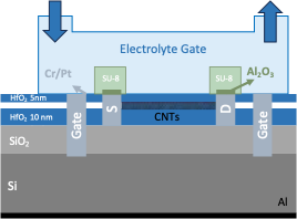
Fig.Thecross-sectionalschematicofCNT-FETafterSU-8andHfO2passivation
Passivation of CNT-FETsusing acombination of SU-8 and HfO2significantlyimprovesdeviceperformance[15].Thisdual-layerapproachresultsin:
- asubstantialreductioninaverageleakagecurrent,
- enhancedstabilityinionicmedia,and
- ahigherfabricationyield(approximately 90%)comparedtonon-passivatedor singly passivated devices.
This strategy leverages the macroscopic insulation of photoresist and the nanoscale protection and gate dielectric enhancement provided by HfO2. This combined barrier effectively minimizes ionic interference whilepreserving thebeneficial attributes of CNT-FETsforbiosensing,suchashighsensitivityandlow-voltageoperation.
1.3.PolymersinFET
Hafnium dioxide (HfO?) passivation layers have proven effective in addressing key challenges of carbon nanotube field-effect transistor (CNT-FET)biosensors, notably mitigating unintended doping effects and enhancing surface stabilitycritical improvements for device performance. Despite these advantages, HfO?is not without limitations. While itexhibits biocompatibility, chemical stability, and low toxicity, its susceptibility to hydrolysis in aqueous and biological environments poses a significant drawback[43].Thishydrolyticinstabilitycompromisesthelong-termreliabilityand
reproducibility of HfO?-based biosensors, ultimately degradingtheir sensitivitya vital parameter for precise analyte detection. Such shortcomings hinder the widespread industrial adoption of HfO?in biosensing applications, underscoring the need for more robust passivation strategies.
To overcome the limitations associated with HfO?passivation layers, polymers have emerged as a promising complementary or alternative material. Polymers bring unique functional versatility andbiocompatibility, makingthemhighlyeffectivefor biomolecule immobilization [20, 44]. Byintroducingactive functional groups,polymer coatings can counteract the inert nature of HfO?, improving biomolecular adhesion [17] and creating a favorable microenvironment for analyte interactions. Additionally, polymersserve asaprotective barrier, preventing hydrolysis oftheunderlying HfO? layer and thereby enhancingthe device's longevity and reliability[16].These properties make polymers avaluable addition to biosensor designs, particularly for applications requiring highsensitivityandstability.
Polymers can be broadly classified into two categories based on their electrical conductivity.
ConductivePolymers(CPs)
CPs, such as poly(3,4-ethylenedioxythiophene):polystyrene sulfonate (PEDOT:PSS), polyaniline (PANI),and polypyrrole (PPy), arewidely used inbiosensors[17, 20], due totheir electrochemical activity, electrical conductivity, mechanical flexibility, and biocompatibility. These materials excel at mediating electron transfer between biomolecules and electrodes, making them ideal for enhancing signal transduction in CNT-FETs[44]. Additionally, their cost-effective and scalable synthesis makes them highlyattractiveforindustrialapplications[45].
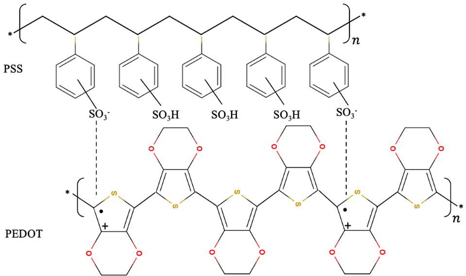
[46]
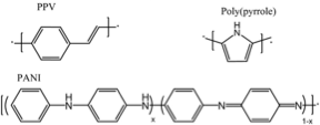
[17]
Non-ConductivePolymers(NCPs)
Although conductivity is a key consideration, NCPssuch as chitosan, gelatin, dextran, cellulose, and polystyrene, playacrucial role inbiosensing byserving assupport matrices for biomolecule immobilization. These polymers are valued for their excellent biocompatibility, low toxicity, and permselectivity, which are essential for maintaining biomolecule functionality and stability insensor environments[47]. Byproviding a stable microenvironment for biomolecules, NCPssignificantly enhance biosensor performance,particularlyincomplexbiologicalmatrices.
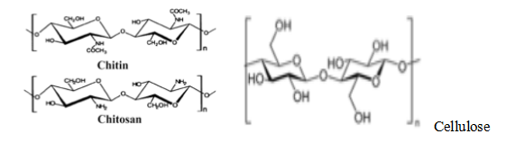
Fig.adaptedfrom[20]
1.4.ImmobilizationStrategiesofBiomolecules
Theimmobilizationofbiomoleculessuchasenzymes,antibodies,nucleic acids,andcells is a crucial factor in determining the performance of biosensors. The effectiveness of immobilizationdependsonselecting amethodthatpreservesthebiomolecule'snativeactivity, ensures proper orientation, and maintains stability under operational conditions, thereby optimizing sensitivity, stability, and longevity [48].
Immobilization techniques are chosen based on the type of biomolecule and its intended application. For example, antibodies and single-stranded DNA (ssDNA) are commonly immobilized through adsorption or covalent/cross-linkingattachment to polymer surfaces, ensuring analyte accessibility to biorecognition sites. This is essential for achieving rapid bindingkineticsinimmunosensorsandnucleicaciddetectionsystems.Incontrast,
oxidoreductaseenzymes, such as glucose oxidase, are typically entrapped within conductive polymer matricesto facilitate efficient electron transfer and catalytic activity.
PhysicalImmobilization
Adsorption
Adsorption isawidelyusedtechnique forimmobilizingbiomolecules,suchasDNA, onelectrode surfaces duetoitssimplicity, cost-effectiveness, and lackofrequirement for chemical reagents or probe modification [49]. This method relies on electrostatic interactionsbetweennegativelychargedbiomoleculesandpositivelychargedfilms. The use of chitosan as a cationic polymeric film has been extensively studied for DNA probe adsorption, owing toitsbiocompatible nature anddense positive charge distribution [50, 51].
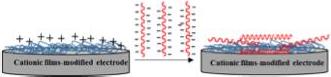
Fig.Aschematic of theDNAprobeimmobilization viaelectrostatic adsorption. [adapted from [49]]
Despite these advantages, the method has significant limitations. The stability of DNA probemonolayers isvulnerable toenvironmental conditions including pH,ionic strength, and temperature variations, while random probe orientation on the electrode surfacecancompromisehybridizationefficiency.
Entrapment
Another type of physical immobilization technique involves trapping enzymes within a polymermatrix,wheretheenzymemoleculesarephysically confined nearthe transducer throughcrosslinked polymerstructures[48,52].Whilethismethodoffers the practical advantages of simple fabrication and cost-effectiveness, the polymernetwork acts as a double-edged sword - it successfully retains the enzymes but simultaneouslycreatesdiffusionbarriersthatcanlimitsubstrateaccessibility, ultimatelyaffectingthebiosensor'ssensitivity.
ChemicalImmobilization
Covalent-Bonding
Covalent immobilization of biomolecules such as DNA and enzymes to the polymers, represents a robust approach characterized by superior binding stability and controlled molecular orientation. This method typically involves strategic modification of biomolecules with functional groups such as thiols (-SH) or amines (-NH2), enabling specificattachmenttofunctionalizedelectrode surfaces[52].Unlikephysical adsorption, covalent bonding ensures precise molecular orientation and prevents desorption, thereby maximizing biosensor performance through reduced non-specific bindingandenhancedsubstrateaccessibility[53].
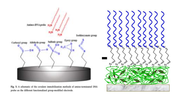
Fig.Schematic ofchemicalbondsin,a)CovalentImmobilization[adaptedfrom[49]] &;b)Cross-LinkingImmobilization[adaptedfrom[54]]
However,thisenhancedstability,andcontrolcomeswithincreasedfabrication complexity, requiring specificchemicalmodificationsandpotentiallylimitingsurface regeneration.Despitethesechallenges,thereduceddiffusionbarriersandimproved molecularorientationmakecovalentimmobilizationparticularlyvaluablefor applicationsdemandinghighsensitivityandreproducibility.
Cross-Linking
Cross-linking immobilization involves theuse of chemical agents, such asglutaraldehyde, to form stable bonds between biomolecules and polymer matrices[55]. Thismethodisclosely related to covalentbonding,asboth rely onchemicalinteractions toachievestronganddurableattachments.Thedistinctionliesintheuseofcross-
linkers,whichserveasmolecularbridgestoconnect biomolecules tothepolymer. While some literature categorizes cross-linking and covalent bonding as distinct techniques [17, 52], others consider them variations of the same approach due to their shared dependence on chemical bonds [49].Cross-linkingimmobilization offers similar advantages and downsides with the requirement of additional step for cross-linker attachment to the polymer.
1.5.Hypothesis
As detailed in the section, the integration of polymers into carbon nanotube field-effect transistor (CNT-FET)-basedbiosensors is hypothesized to enhance their sensitivity, stability and biocompatibility. Polymers withtailored mechanical, chemical, andelectrical properties are expected to address limitations in traditional CNT-FET biosensors, such as drift in sensitivity, biomolecule immobilization, and environmental degradation.
This master thesis explores the following research questions to investigate the role of polymer-mediatedimprovementsinbiosensorsdesignedforDNAorantibody detection:
- Whichpolymers can be usedto chemically immobilize thebiomolecules, DNAandenzyme,havingamine(-NH2)groupatend?
- Whatdepositiontechniquescanachieveuniformthinpolymerfilmsinthe nanometerrangeonCNT-FETswithoutdamagingtheunderlyingstructure?
- Howdodifferentpolymerproperties(e.g.,conductivityorbiocompatibility) influencethesignaltransductionefficiencyinCNT-FETbiosensors?
- CantheuseofpolymersextendtheoperationallifespanofCNT-FET biosensors by reducing material degradation or fouling during prolonged use?
- Whatpolymer designstrategies yield thebestperformance improvements for biosensorswhenevaluatedforclinicalordiagnosticapplications?
1.6.OverviewofThisThesis
This master thesis consists of the following main chapters: Chapter 1 provides an introduction to CNT-FETsas biosensors, discussing their working principles, different configurations,andlimitations. Italso highlightstherole ofpolymers forpassivation and various biomolecule immobilization strategies. The chapter concludes with the research hypothesis and an outline of the thesis. Chapter 2 describes the materials and methods used, including CNT-FETfabrication, polymer synthesis and deposition, film characterization, microfluidics integration, and biomolecule immobilization techniques. Chapter3presents theresults anddiscussion, focusing ontheperformance ofCNT- FETs with polymer passivation and immobilized biomolecules. Finally, Chapter 4 discusses thestrengthsandlimitationsofthepresented work,alongwithfuture prospectsfordevelopingadvancedCNT-FET-basedbiosensors.
- MaterialssMethods
Inthischapter,theexperimentalmethodsandusedmaterialsarebrieflydescribed.
2.1.CNT-FETFabrication
The fabrication method was same as used by Leticia et al. 2024 [16]. The field-effect transistor sensors were fabricated on a highly doped Si/SiO2wafer with a hafniumoxide (HfO2) layer deposited via atomic layer deposition. The semiconducting single-walled carbon nanotubes were integrated from acommercial dispersion (Nanointegris IsoSol- S100) using a printing technique and subsequently patterned through oxygen plasma etching.Thecarbon nanotubes werecontacted usingelectronbeamlithography, followed by ion-beam sputter deposition of chromium/platinum/aluminum oxide (Cr/Pt/Al2O3) and a lift-off procedure. After thermal annealing, the devices were encapsulated with 5 nm of HfO2. To enable local liquid-gating through the wafer's backside,wet etching wasemployed to create openings for silicon contacts,which were then covered with Cr/Pt.Source and drain electrode passivation with SU-8 photoresist. The final fabrication step involved mechanically scratching the wafer's backside and depositing aluminum via physical vapor deposition to establish electrical contact. The schematicstructureoftheCNT-FET deviceusedinthisstudyisshowninFig.1.
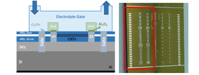
Fig.Schematica)cross-sectionandb)top-viewofaCNT-FET
2.2.PolymerSynthesis
Inthis study, a range ofconductive and non-conductive polymers wereutilized, including poly(3,4-ethylenedioxythiophene):poly(styrenesulfonate) (PEDOT:PSS), polyaniline (PANI),polypyrrole (PPy), polyethylene glycol (PEG), and chitosan. PEDOT:PSSand PANIwere sourced fromabcr GmbH, while chitosan powder and the pyrrole monomer were obtained from TCI Chemicals. Silane-functionalizedPEG was procuredfrom Sigma-Aldrich. Notably, PPywasthe solepolymer synthesizedin-house using establishedprotocols[56].
PPYSynthesis
PPywas synthesized usinga method adapted from Shahryari et al. (2021). Ina typical procedure,1.38mL of Pymonomerwasfirstdissolvedina 100mL mixture ofmethanol anddeionized water(1:1v/v)underconstant stirringuntilaclear,homogeneous solution formed. Separately, 1.62 g of iron(III)chloride (FeCl3), acting as an oxidizing agent,wasdissolvedin120 mL of deionizedwater.This FeCl3solutionwas then slowly introduced intothePy-containing solventmixturetoinitiatepolymerization. The reaction wasallowed toproceed for 24hours atroom temperature (25C) with continuous mechanical agitation.
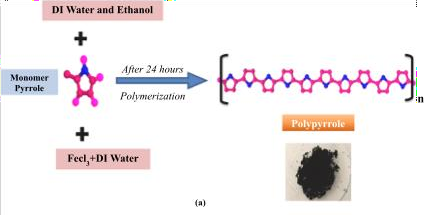
Fig.SchematicoftheunderlyingreactionintheformationofPPy.[56]
After polymerization, the resultingPPy were isolated byfilteringusingfilter paper and washedmultipletimeswitha1:1ethanol-water solution toeliminateunreacted FeCl3andother impurities. Thepurified PPyproduct wassubsequently dried inanovenat 60Cfor24hours,yieldingafineblackpowder withamassofapproximately255mg.
The final products dark coloration and powdery consistency confirmed successful synthesis,aligningwithestablishedcharacteristicsofconductivePPy.
2.3.PolymerDeposition
Spin-coating
Spin-coating is a widely utilized technique in materials science, particularly for the deposition of thin and uniform polymer films on flat substrates [57].Itssimplicity,cost- effectiveness, and versatility have established it as a standard method in both academic research and industrial applications, with significant relevance in fields such as microelectronics,photonics,andbiomedicaldevices.
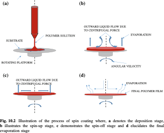
Fig.Processofspin-coating[adaptedfrom[57]]
The spin-coatingprocess, shown in Fig., operates by harnessingthe centrifugal force generated during the high-speed rotation of a substrate, which facilitates the uniform spreading of a liquid solution across its surface. Typically, apolymer solution composedof apolymer dissolvedinavolatilesolventisdispensedat thecenter of the
substrate. As the substrate rotates, the solution spreads radially outward under the influenceofcentrifugalforces. Concurrently, thevolatilesolventevaporates, resulting in the formation of a thin polymer film.
Thethickness of the resulting film isinfluenced by several critical parameters,including spin speed, solution viscosity, polymer concentration, solvent volatility, and spin time. Theseparameters were initially determined based on a review of existingliterature and further refined experimentally to achieve optimal uniformity, as observed under optical microscopy. The final parameter optimization was conducted to ensure the desired film thickness and uniformity for the specific polymer under investigation. Theoptimized spin-coatingparametersforthedepositedpolymersaredetailedbelow.
Table.Spin-coatingparametersforthedepositedpolymers.
|
Polymer |
Solution |
Spin-coating Parameters |
Post-coating Treatment |
Ref. |
|
PEDOT:PSS |
Commercial solution |
10003000 rpmfor40s* |
Annealed at 135C for 1h, washed with DI water |
[58] |
|
PANI |
10mg in 4mL m-cresol, stirred for 5h |
10003000 rpmfor60s |
Dried at 60C for 5 min |
[59] |
|
PPY |
Dissolved in m- cresol, stirredfor 4-5 days |
10003000 rpmfor60s |
Dried in air at 60 min |
[60] |
|
Chitosan |
0.15g in 15mL water with 2?etic acid, stirred 10-15 min |
30005000 rpmfor60s |
Dried at 25C overnight, washed with NaOH, dried in nitrogen |
[54] |
*Substratewastreatedwithozoneplasmafor5min.
Grafting(PEGDeposition)*
Toprepare thesolution,polyethyleneglycol (PEG)isfirstdissolved ineithertoluene or amixture ofethanol and deionized water (EtOH:DI).Thisisdone using avortex mixer,whichrapidlyspinsthemixturetoensureitbecomeswell-mixedand
homogeneous. Before applying the PEG,the carbon nanotube field-effect transistors (CNT-FETs)are treated with ozone plasma for five minutes at room temperature.This step iscrucial as it activates the surface, making it more reactive and ready for the polymer to attach effectively.
Oncethe PEGsolution is ready,itis carefully applied to thesubstrate and leftto incubate for an hour.This allows the PEGto spread evenly and forma consistent layer. After incubation,thesubstrateis rinsed with the original solvent to wash away any PEG molecules that didnt bind properly. Finally, the functionalized CNT-FETsare dried gentlyunder astream ofnitrogen gas.Thisensures thepolymerlayer remainsstable andintact,providingareliablesurfaceforfurtheruse.(Addreferenceandalsoimage)
*Missingreference,Iwasntabletofindtheref.
2.4.PolymerFilmCharacterization
Bright-fieldMicroscopy
Bright-field microscopy is a valuable technique for examining the morphology of thin polymer layers, particularly for assessing layer uniformity and identifying defects[61]. Thismethodallowsresearchers tovisualizesurfacefeaturesandstructural characteristics of polymer films without the need for complex sample preparation or labeling. By illuminating the sample with white light and collecting the transmitted or reflected light,bright-field microscopy can reveal variations insurface roughness, andthepresence of imperfections such as cracks,bubbles,orparticulate contamination.The contrastinbright-fieldimagesarisesfromdifferencesinlightabsorption, refraction, and reflection across the sample, enabling the detection of subtle morphologicalvariationsinthepolymer layer. Thistechniqueisparticularly useful for rapidscreening of large sample areasand can provide importantinsightsinto the quality and consistency of polymer coatings or thin films. While bright-field microscopy has limited resolution compared to electron microscopy techniques, it remains a crucial tool for initial characterizationandqualitycontrolinpolymerscienceandengineering.
AtomicForceMicroscopy(AFM)
Atomic Force Microscopy (AFM) serves as a powerful and versatile technique for characterizingpolymer thin films, offering precise measurements of both film thickness and surface smoothness. The thickness measurement employs a controlled scratching method, wherein a portion of the organic layer is carefully removed using a needle to createastep[62,63].AFMthenscansacrossthisartificially created step,measuring theheightdifference between the substrate and the filmsurface.Thisapproach provides
direct,localizedthicknessmeasurementswithnanometer-scaleprecision,applicableto a wide range of film thicknesses.
Concurrently, AFMassesses surface smoothness by analyzing topographical data to calculate parameters such as root mean square roughness. The high-resolution imaging capability of AFM,coupled with its non-destructive nature (outside the intentionally scratched area), makes itparticularly suitable for characterizingdelicate polymer layers. However,caution mustbeexercised during thescratching process toavoiddamaging theunderlyingsubstrate,whichcouldcompromisemeasurementaccuracy.
The dual capability of AFMto provide both thickness and roughness data in a single measurement renders it an invaluable tool for polymer thin film characterization across various applications, from electronics tobiomedical devices. Thismethod'sabilityto offerdirect, physical measurementswithoutrelying oncomplexmodelingor assumptionsfurtherenhancesitsutilityinresearchanddevelopmentsettings .
2.5.Microfluidics
A custom-designed polydimethylsiloxane (PDMS) microfluidic channel was created to precisely deliver biological or pHsolutions to thesensing area. Thechannel maintains theelectrical isolation oftheelectrodes andpreventsliquiddamage.ThePDMS materialisidealforthisapplication becauseitistransparent, biocompatible, and flexible,making it easy to attach to the CNT-FET.This setup,as shown in Fig.,allows for a controlled microenvironment, which improves the accuracy and consistency of electrochemical measurements.
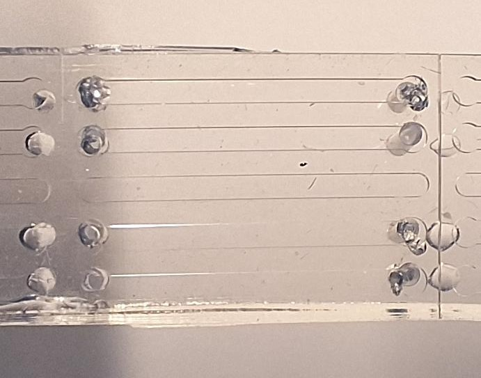
Fig.Top-viewofthePDMSchannelusedformicrofluidics.
2.6.ElectricalMeasurementsofCNT-FETDevice
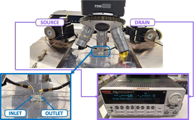
Fig.Thesetupforelectricalsignalmeasurements.
In this study, we characterized the electrical properties of CNT-FETdevices using a Keithley 2636B SourceMeter. The setup, as shown in Fig., included a microscope to assist in aligning and attachinga PDMSmicrofluidic channel to the chip.Thechannel, fitted with inlet and outlet pipes, wassecurely bonded to prevent leaks. Solutions were introducedviaasyringe,ensuringthechannel wasfullyfilledbeforemeasurements. Themicroscope also helped monitor theprocess,preventingspills or contact withthe source/drainelectrodesandensuringproperelectricalconnections.
Gate voltage (Vg)sweeps from -0.5 V to 0.8 V were applied at a fixed drain-source voltage (Vds)of-0.1V.Thisallowed ustocollect pulsed transfer characteristics and gatecurrent measurements, providing insightsintothedevices dynamic performance and gate leakage. We extracted key parameters such as threshold voltage, transconductance, andon/offcurrentratios,providing acomprehensiveunderstanding of the CNT-FET devices electrical performance. To ensure the accuracy and reproducibility of our findings, we measured each device three times for every measurement,ensuringconsistencyandreliabilityinourresults.
2.7.BiomoleculeImmobilization
Allthepolymers selected wereselected onthecriteria whethertheyhaveinherent ability to form any of the covalent bond which can help us achievevery high sensitivity withLODmatchingthediagnosticsgoldstandardsoftheparticulardisease.
PEDOT:PSS
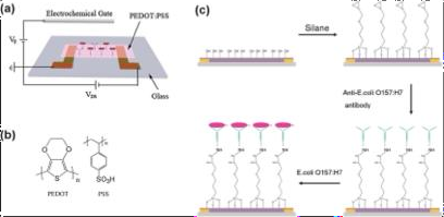
Fig.Processofbiomoleculeimmobilization[adaptedfrom[64]]
Theimmobilization protocol followed the method described byHeet al.,2012[64]. First, PEDOT:PSSactive layers were exposed to oxygen plasma (12 W power) for defined durations to activate the surface. Subsequently, the devices were incubated in a 1.5%(v/v) 3-glycidyloxypropyltrimethoxysilane (GPMS) toluene solution for 12 hoursto facilitate silane functionalization. After silane grafting, the devices were rinsed twice withtoluene and ethanol to removeunbound residues and then thermally cured at 100C for 4 hours to stabilize the surface. For antibody conjugation, 40 ?L of anti-E. coli O157:H7antibody solution (0.1mgmL??1;inphosphate-buffered saline,PBS)was applied to the PEDOT:PSSchannel and allowed to bind for 10 hours.Finally,unbound antibodies were removed by washing the devices sequentially with PBSand deionized water.
PANI
The PANI-coatedfilter papers were functionalized for antibody immobilization using glutaraldehyde as a crosslinker [65]. First, substrates were treated with 1% aqueous glutaraldehyde to activate PANIssurface amine (NH?)groups via covalent bonding, leaving free aldehyde (CHO)termini for subsequent biomolecule conjugation. After rinsing to remove excess glutaraldehyde, target-specific antibodies (monoclonal anti- MPOor polyclonal anti-Myoglobin) were applied to the sensor region. The aldehyde groupsreactedwithlysineresiduesontheantibodies,enablingcovalentattachment.
Unbound siteswere blocked with bovine serum albumin (BSA)to minimize nonspecific interactions. This stepwise approachsurface activation, antibody coupling, and blockingensured selective andstableimmobilization ofbiorecognition elementson thePANIplatform,criticalforbiosensingapplications.
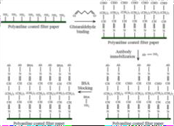
Fig.BiomoleculeimmobilizationonPANI-coatedpaper.[65]
PPY
Tran et al. 2014 [66] immobilized thiol-terminated DNA probes on polypyrrole (PPy). However, this approach is incompatible with amine-terminated probes or antibodies. While literature on immobilization of amine-ended biomolecules on PPy islimited, its structural similarity to PANIin having free -NH2groups, it was hypothesized that a similarapproachcouldbeadaptedforbiomoleculeimmobilizationontoPPy.
Chitosan
Chitosan-modifiedelectrodeswerefunctionalizedwithamine-terminatedssDNA probesusingglutaraldehydecrosslinking[54].First,thechitosansurfacewasactivatedbyimmersionin1%glutaraldehydefor2hours,enabling covalentbonding between chitosans amine groups and thecrosslinkers aldehyde termini. After rinsing,30?Lof0.5M ssDNAprobesolutionwasappliedtothe activatedsurfaceand incubatedfor1houratroomtemperature(25C),facilitatingcovalentattachmentof theDNAviaitsterminalaminegroups. Unboundprobeswereremovedbythorough washing.
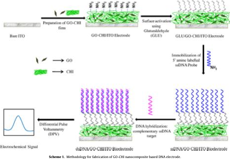
Fig.ssDNAimmobilizationonChitosan-grapheneelectrode
Given that silated-PEG inherently possesses free silane groups, biomolecules can be immediately immobilized onto the surface following PEG deposition without further modification.
*Needproperreference.
References
- Li,,et al., TowardtheCommercializationof CarbonNanotubeFieldEffect TransistorBiosensors.Biosensors(Basel),2023.13(3).
- Bier,F.andS.Schumacher, IntegrationinBioanalysis: Technologies for Point-of-CareTesting.MolecularDiagnostics,2013.
- C,,et al., Multiplexed Point-of-Care Testing - xPOCT - PubMed. Trends inbiotechnology, 2017 Aug. 35(8).
- Lu,,etal., Nanomaterial-basedbiosensorsformeasurementoflipidsand lipoproteinstowardspoint-of-careofcardiovasculardisease.Analyst, 2017/09/08. 142(18).
- H,,etal., Adielectric-modulatedfield-effecttransistorforbiosensing- PubMed.Naturenanotechnology,2007Jul.2(7).
- B,,F.E,andB.PV,Fieldeffect sensorsfor nucleicAciddetection: recent advancesandfutureperspectives-PubMed. Sensors(Basel, Switzerland), 05/04/2015. 15(5).
- Gupta, S.,Sharma,and R.S.Verma,Polymers in biosensor devices for cardiovascular applications. Current OpinioninBiomedicalEngineering, 2020. 13: p. 69-75.
- Yao,,etal., CarbonNanotubeField-EffectTransistor-BasedChemicaland BiologicalSensors.Sensors(Basel),2021.21(3).
- Shkodra,,etal.,Electrolyte-gatedcarbonnanotubefield-effecttransistor- based biosensors: Principles andapplications.AppliedPhysicsReviews,2021. 8(4).
- Y,,etal., Two-DimensionalMetal Nanomaterials: Synthesis, Properties, and Applications-PubMed.Chemicalreviews,07/11/2018.118(13).
- Subramanian, S.,et al., Rapid, sensitive and label-free detection of Shiga-toxin producing Escherichia coli O157 using carbon nanotube biosensors. Biosensors andBioelectronics,2012/02/15.32(1).
- Simon, J., et al., Overview of Carbon Nanotubes for Biomedical Applications. Materials2019, Vol. 12, Page624, 2019-02-20. 12(4).
- Kim,, et al., Recognition of Single Mismatched DNA Using MutS- ImmobilizedCarbonNanotubeFieldEffectTransistorDevices. TheJournalof PhysicalChemistryB, August17, 2009. 113(36).
- Albarghouthi, F.M.,et, Addressing SignalDriftandScreening forDetection ofBiomarkerswithCarbonNanotubeTransistors.ACS Nano,2024.
- Albarghouthi, F.M.,et al., Passivation Strategies for Enhancing Solution-Gated CarbonNanotubeField-EffectTransistorBiosensing PerformanceandStability inIonicACSApplNanoMater,2022.5(10):p.15865-15874.
- AlvesdaSilva,,M.Hartmann,andS.Hermann,Polymer-MediatedIncrease inSensitivityandStabilityofCNT-FETpHSensor,inEurosensors 2023.2024.
- Bhattacharjee, M. and Bandyopadhyay, ConductivePolymer Nanobiosensors.EnvironmentalNanotechnologyVolume5,2021.
- Ghadimi, H., S. Ab Ghani, and I.S. Amiri, Introduction, in Electrochemistry of Dihydroxybenzene2017.p.1-30.
- Ghorbani Zamani, F., et al., Current trends in the development of conducting polymers-basedTrACTrendsinAnalyticalChemistry,2019.118:
- 264-276.
- Long,J.,et al., Polymers in Biosensors, in Multifaceted Protocol inBiotechnology. 2018. p. 151-165.
- Luong,H.T.,et al.,Recent Advances of Conducting Polymers and Their CompositesforElectrochemicalBiosensing Applications. JFunctBiomater, 2020. 11(4).
- DE,,et al.,Structural absorption by barbule microstructures of super black birdofparadisefeathers-PubMed.Naturecommunications,01/09/2018.9(1).
- N,,C.R,andW.Q,Recent AdvancesinElectric-Double-LayerTransistors forBio-ChemicalSensingApplications-PubMed.Sensors(Basel, Switzerland), 08/05/2019. 19(15).
- S,,J.YS,andK.HK,Metal-oxide-semiconductor field-effect transistorwith avacuumchannel-PubMed.Naturenanotechnology,2012Aug.7(8).
- Tambekar, M.R.,R.Nade, and A. Gajarushi, Analysis of back gate and gateallaroundCNTFETstructure, inProceedingsoftheInternationalConference &WorkshoponEmerging TrendsinTechnology. 2011, Associationfor ComputingMachinery:Mumbai,Maharashtra,India.p.11441147.
- Srimani, T., et al., 30-nm Contacted Gate Pitch Back-Gate Carbon Nanotube FETsfor Sub-3-nm Nodes | IEEEJournals & Magazine | IEEE Xplore. IEEE TransactionsonNanotechnology,18.
- N, B., et al., Label-free disposable immunosensor for detection of atrazine - PubMed. Talanta, 2016. 146.
- Cho,-K.andW.-J. Cho, Ultra-highsensitivitypH-sensorsusing silicon nanowirechanneldual-gatefield-effecttransistorsfabricatedbyelectrospun polyvinylpyrrolidonenanofiberspatterntemplatetransfer.Sensorsand ActuatorsB:Chemical, 2021/01/01. 326.
- Ahn,-H.,B.Choi,andS.-J. Choi,Understanding thesignal amplificationin dual-gateFET-basedbiosensors.JournalofAppliedPhysics,2020/11/14. 128(18).
- N,,etal., Aptamer-field-effecttransistorsovercomeDebyelength limitationsforsmall-moleculesensing -PubMed. Science(New York, N.Y.), 10/19/2018. 362(6412).
- F,,etal., Real-TimeMonitoring ofCellularCultureswithElectrolyte-Gated CarbonNanotubeTransistors-PubMed. ACS appliedmaterials& interfaces, 10/16/2019. 11(41).
- Joshi, S.,et, FlexibleLactateandGlucoseSensorsUsing Electrolyte-Gated CarbonNanotubeFieldEffect TransistorforNon-InvasiveReal-Time Monitoring | IEEEJournals & Magazine | IEEEXplore. IEEESensors Journal, 2017. 17(14).
- Alabsi, S.S.,et al., AReview of Carbon Nanotubes Field Effect-BasedIEEEAccess,2020.8:p.69509-69521.
- Albarghouthi, F.M.,et al., Passivation Strategies for Enhancing Solution-Gated CarbonNanotubeField-EffectTransistorBiosensing PerformanceandStability inIonicACSAppliedNanoMaterials,October4,2022.5(10).
- Sinha, S.andPal,Acomprehensivereview of FET?basedpH sensors: materials,fabricationtechnologies,andmodeling.ElectrochemicalScience Advances, 2022. 2(5):p. 2100147.
- Xu, K., et al., Electric-double-layer-gated transistors based on two-dimensional crystals: recent approachesand JournalofPhysics:Materials, 2020- 05-04. 3(3).
- Hu,,D.S.Hecht, and G. Grner, Carbon Nanotube Thin Films: Fabrication, Properties,andApplications.ChemicalReviews,July22,2010.110(10).
- Oldham, K.B., A GouyChapmanStern model of the double layer at a (metal)/(ionic liquid) interface. Journal of Electroanalytical Chemistry, 2008/02/15. 613(2).
- Torricelli,,etal.,Electrolyte-gatedtransistorsforenhancedperformance bioelectronics.Naturereviews.Methodsprimers,2021Oct7.1(1).
- Svetlova, A., et al., Origins of Leakage Currents on Electrolyte-Gated Graphene Field-Effect Transistors. ACS Applied Electronic Materials, November 23, 2021. 3(12).
- Meng,,etal., Hafnium oxide layer-enhanced single-walled carbonnanotube field-effecttransistor-basedsensing platform.AnalyticaChimicaActa, 2021/02/22. 1147.
- Kesler, V.,Murmann, and H.T.Soh,Going beyond the Debye Length: Overcoming ChargeScreening LimitationsinNext-GenerationBioelectronic Sensors. ACSNano, 2020Nov23. 14(12).
- Siboro, P.Y.,et al.,Harnessing HfO2 Nanoparticles for Wearable TumorMonitoring andSonodynamicTherapyinAdvancing Cancer ACS Nano, January 10, 2024. 18(3).
- Ramanavicius, S. andRamanavicius, Conducting PolymersintheDesignof BiosensorsandBiofuelCells.Polymers(Basel),2020.13(1).
- Balint, R.,J.Cassidy, and S.H.Cartmell, Conductive polymers: Towards a smartbiomaterialfortissueengineering. ActaBiomaterialia, 2014/06/01. 10(6).
- Mikaeeli, A., et al., Electrical Characterization of Cu-Doped PEDOT:PSS Polymeric Thin Films. Engineering Proceedings 2023, Vol. 56, Page 327, 2023-11-07. 56(1).
- M,,J. C,andX.W,Usingelectropolymerizednon-conducting polymersto develop enzyme amperometricbiosensors-PubMed.Trendsinbiotechnology, 2004 May. 22(5).
- Lakard, B.,ElectrochemicalBiosensorsBasedonConducting Polymers:A Review.AppliedSciences, 2020. 10(18).
- Rashid, J.I.A.and N.A.Yusof, The strategies of DNA immobilization and hybridization detection mechanism in the construction of electrochemicalDNAsensor:ASensingandBio-SensingResearch,2017.16:p.19-31.
- Taufik, S.,et al.,BismuthOxideNanoparticles/Chitosan/Modified Electrode as BiosensorforDNAInternationalJournalofElectrochemical Science, 2011/06/01. 6(6).
- Qi, X., et al., Electrochemical DNA biosensor with chitosan-Co3O4 nanorod- graphene composite for the sensitive detection of staphylococcus aureus nucgeneBioelectrochemistry,2012/12/01.88.
- Sassolas, A., L.J. Blum, and B.D. Leca-Bouvier, Immobilization strategies to developenzymaticBiotechnologyAdvances,2012/05/01.30(3).
- Lu, Z., et al., Covalently linked DNA/protein multilayered film for controlled DNAJournalofColloidandInterfaceScience,2007/10/01.314(1).
- Singh,,etal., Grapheneoxide-chitosannanocompositebased electrochemicalDNA biosensorfordetectionoftyphoid.Sensorsand ActuatorsB:Chemical, 2013. 185:p. 675-684.
- Wang,,et al.,Hybridization biosensor based on the covalentimmobilization ofprobeDNAonchitosanmutiwalledcarbonnanotubesnanocompositeby using glutaraldehydeasanarm linker. SensorsandActuatorsB:Chemical, 2011/08/01. 156(2).
- Shahryari, Z.,et, Corrosionmitigationabilityofdifferentlysynthesized polypyrrole (PPy-FeCl3 & PPy-APS)conductive polymers modified withNa2MoO4onmildsteel in3.5% NaCl solution: Comparativestudyand optimization.CorrosionScience,2021.193.
- Das,andA.Chanda,FabricationandPropertiesofSpin- CoatedPolymerFilms,inNano-sizePolymers.2016.p.283-306.
- Kawamura, R. and T. Michinobu, PEDOT:PSSversus Polyaniline: AComparativeStudyofConducting PolymersforOrganicElectrochemical Transistors.Polymers(Basel),15(24).
- Jarad, A.N.,Ibrahim, andN.M.Ahmed, Synthesisandcharacterizationthin filmsofconductivepolymer(PANI)foroptoelectronicdeviceapplication. 2016.
- Sakthivel, S. andBoopathi, Synthesisandcharacterizationofpolypyrrole (PPy)thinfilm byspincoating Technique. J. Chem. Chem. Sci, 2014. 4:p. 150-155.
- Gutierrez-Medina,,Opticalsectioning ofunlabeledsamplesusing bright- fieldmicroscopy.ProcNatlAcadSciUSA,2022.119(14):p.e2122937119.
- Rahman, M.U.,et al., Dynamics andStructureFormationof ConfinedPolymer ThinFilmsSupportedonSolidPolymers(Basel),2021.13(10).
- Vasi?, B.andAkrabi?, Thicknessmeasurementofthinfilmsusing atomic forcemicroscopybasedscratching. SurfaceTopography:Metrologyand Properties, 2024. 12(2).
- He,-X.,etal., Detection ofbacteria with organicelectrochemical transistors. JournalofMaterialsChemistry,2012.22(41).
- Mondal, D.,Paul,andS.Mukherji, ImpedanceSpectroscopy-Based Detection of Cardiac Biomarkers on Polyaniline Coated Filter Paper. IEEESensorsJournal,2017.17(16):p.5021-5029.
- Tran, T.L.,et al., Effective immobilization of DNA for development of polypyrrole nanowires based biosensor. Applied Surface Science,314: p. 260-265.